The IEEE 802.3bs 200GbE and 400GbE Architecture
The development of the underlying architecture that will be the foundation of a new Ethernet rate family is perhaps the most crucial aspect of such a project. The architecture must be flexible and be able to scale to support future standards and technology developments. Additionally, the industry expects that any deployed systems, based on the existing standard, will be upgradeable to support any future family members. And with it being Ethernet – the expectation is that the architecture would be cost effective to develop, deploy, and would enable multi-vendor interoperability.
With the IEEE 802.3bs™ standard, the task force participants recognized upfront that they needed to define an architecture to support at least three generations of electrical and optical signaling in the immediate future, providing effective building blocks at 25 Gb/s, 50 Gb/s, and 100 Gb/s lane rates. It also anticipated that the industry would expect physical layer specifications for carrying 200 Gb/s and 400 Gb/s Ethernet across printed circuit board traces, backplanes, copper twin-ax cables, multi-mode fiber, as well as single mode fiber from 500m to reaches spanning as far as perhaps 40 to 80km.
Figure 1 illustrates the overall IEEE P802.3bs architecture supporting both 200GbE and 400GbE. Each rate includes a Physical Coding (PCS) sub-layer and a Physical Medium Attachment (PMA) sub-layer, and multiple Physical Medium Dependent (PMD) sub-layers. These three blocks together form a “PHY” to support each of the different media and reaches noted previously.
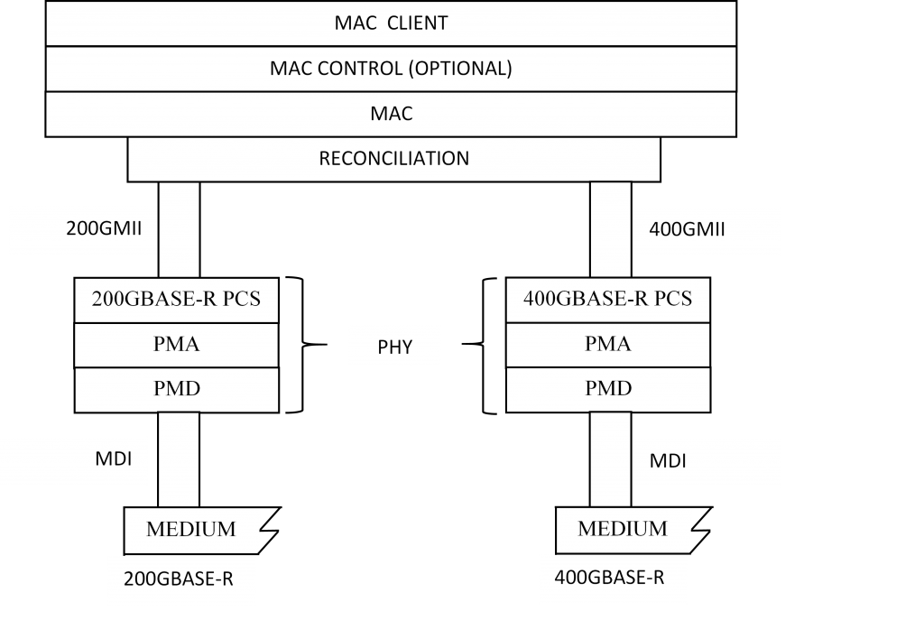
Figure 1- IEEE 802.3bs 200 GbE and 400 GbE Architecture
While the most elegant solutions are often the most simple, the true complexity may be hidden in the simplicity. Some past Ethernet standards employed optional forward error correction (FEC), which would show up in these types of diagrams as a separate sublayer. In the 802.3bs architecture, all PHYs employ Reed Solomon FEC, embedded in the respective PCS layer for each rate. This FEC was selected after considering the trade off between latency and signal gain deemed necessary for both the electrical interfaces and respective optical PHYs defined as part of the 802.3bs standard.
But the decision to embed the FEC in the PCS forced the Task Force participants to develop the 200GbE and 400GbE Extender Sublayers in order to allow the future development of future PCS sublayers that, for example, might employ a new FEC with greater signaling gain for more challenging physical layer specifications.
And that will get covered in the next blog…